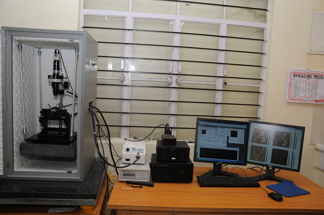
Atomic force Microscope
Technical and Characterization Specifications:
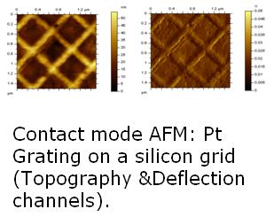
- Contact Mode AFM & F-Z spectroscopy for topography imaging and force measurements
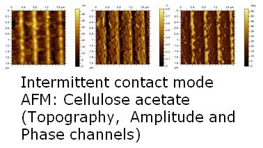
- Intermittent Contact Mode AFM & F-Z spectroscopy
- Scanning Tunneling Microscopy & Spectroscopy
- Kelvin Probe Microscopy for mapping surface potential
- Magnetic Force Microscopy for mapping magnetic domains
- Electric Force Microscopy for mapping electric field gradient
- Current Sensing Atomic Force Microscopy & I-V spectroscopy for mapping current
- Piezoresponse force microscopy and spectroscopy
- Nanolithography for patterning nanometer-scale structures
- Sample types: Thin films, polished solids, dispersed powders on substrates like silicon, HOPG, Au/mica, quartz
- Sample dimensions: X,Y (max) 20mm, 35mm for ambient AFM imaging, XY (max) 20mm for liquid cell AFM imaging
- Top down multipurpose closed loop large scanner (XY 90μm, Z 8μm), resolution for small area scans <500nm x 500nm, with interchangeable nose-cones for STM, AFM, CSAFM, AC-AFM
- Top down multipurpose open small scanner (XY 9μm, Z 2μm), provides atomic resolution, with interchangeable nose-cones for STM, AFM, CSAFM, AC-AFM.
- Scanners compatible with environmental and temperature control options
- STM scanner (XY 10 μm, Z 1.6 μm)
- AFM head with easy laser alignment and high resolution CCD camera
- Vibration and acoustic isolation chamberHeating sample stage (up to 250°C)
- Liquid cell imaging
- Environmental control chamber
- PicoView software capable of real-time 3D data rendering
- PicoImage software for analysis and post-processing images
- PicoLith software for nanolithography