Resistive switching behaviour of RF magnetron sputtered ZnO thin films
R. Rajalakshmi and S. Angappane
AIP Conf. Proc. 1665, 080051 (2015)
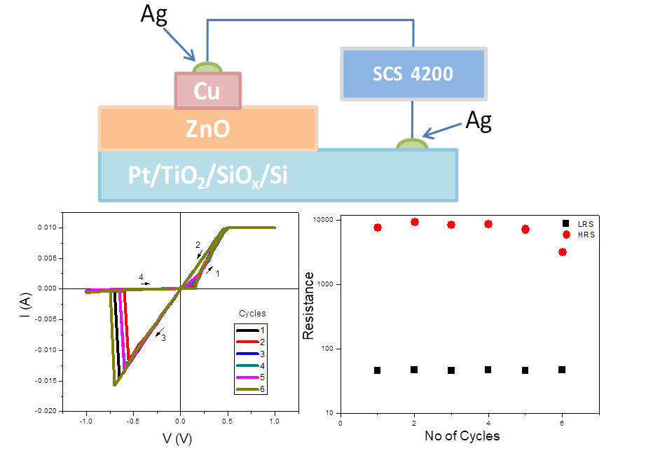
(a) Schematic of Cu/ZnO/Pt device, (b) I-V characteristics and (c) Retention characteristics of our Cu/ZnO/Pt device.
This work involves the fabrication of Metal/ZnO/Pt device and study of resistive switching behaviour. The ZnO films were deposited on Pt/Si substrates by using RF magnetron sputtering and the top electrodes, such as, Cu, Al etc were deposited by DC sputtering. The schematic diagram of a Cu/ZnO/Pt device fabricated for resistive switching studies is shown in figure 1(a). Typically, we observe a small hysteresis loop in the positive cycle and no switching is seen, as shown in figure 1(b). When the voltage is swept from 0 to 1 V in negative cycle, the current sharply jumps to lower values at around 0.6 V, which indicates the switching from LRS to HRS. During the next sweep in positive cycle, the device changes state from HRS to LRS, without sharp switching.
With the negative bias at lower voltage regime, the device exhibits a Ohmic conduction which is due to the formation of filamentary conduction path generated out of oxygen vacancies from bottom electrode to the top electrode. At higher voltage regime, the switching from LRS to HRS is governed by Poole-Frenkel emission. The rupturing of the filaments occurs due to intense Joule heating. Figure 1(c) shows retention characteristics of our Cu/ZnO/Pt device read at 0.25 V, which indicates the HRS to LRS resistance ratio of ~ 200.